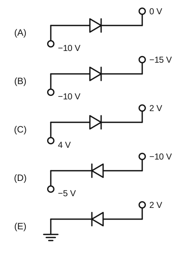
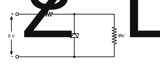
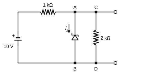
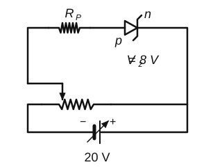
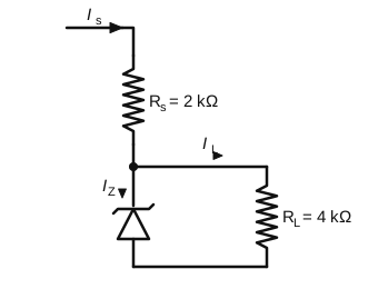
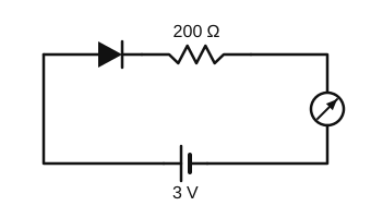
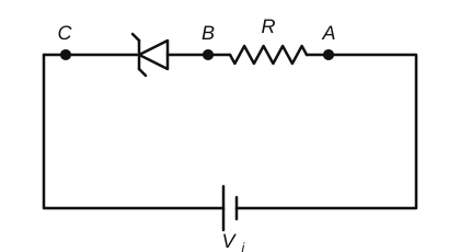
An ideal Zener diode with breakdown voltage of $-3$ V is reverse biased with a negative input voltage $V_i = -5$ V. The magnitude of voltage difference between points $B$ and $A$ is :
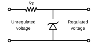
The reverse-biased Zener is in breakdown, since $5\ \text{V} > 3\ \text{V}$. An ideal Zener then holds a constant $3$ V across itself (between C and B).
The rest of the supply voltage appears across the resistor R, which lies between B and A: $$|V_B - V_A| = 5 - 3 = 2\ \text{V}$$
Solution by Sreeraj P, M.Sc Physics
Q 12-14-002NEETNEET 2026Top questionHard
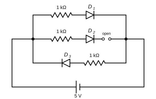
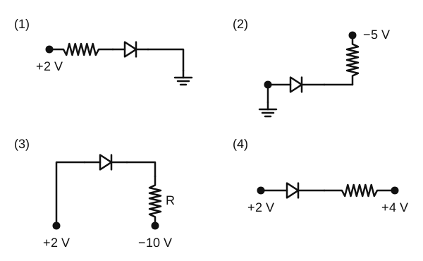
Three identical p-n junction diodes $D_1$, $D_2$ and $D_3$ are connected across a battery as shown in the figure. If the width of the depletion regions of $D_1$, $D_2$ and $D_3$ are $W_1$, $W_2$ and $W_3$, respectively, then the correct option is :
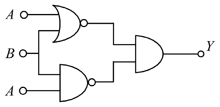
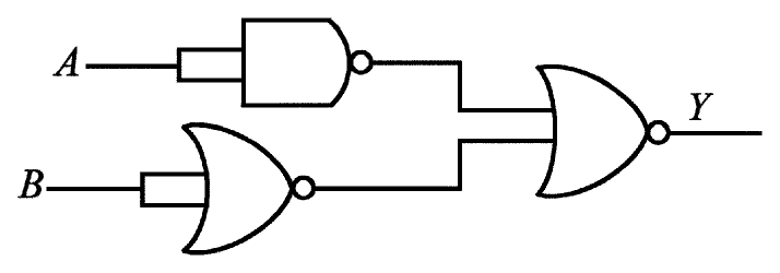
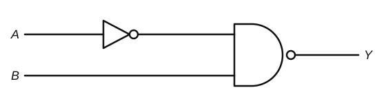
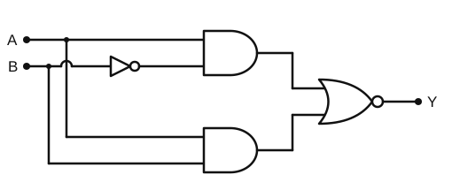
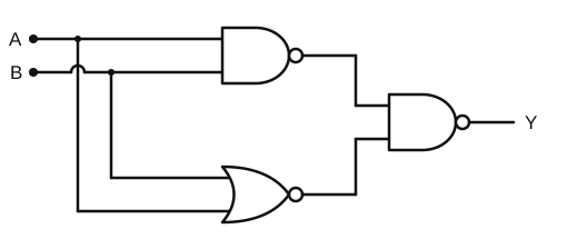
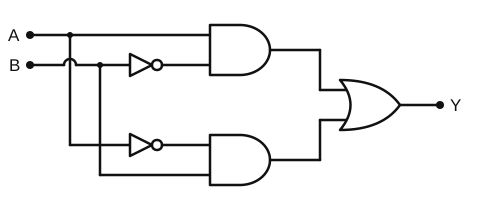
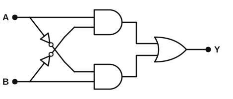
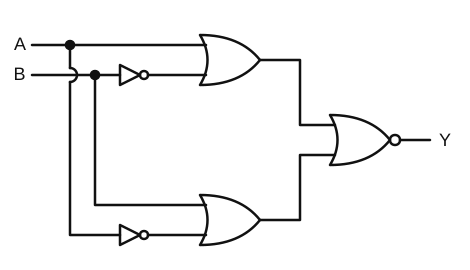
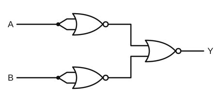
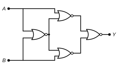
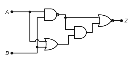
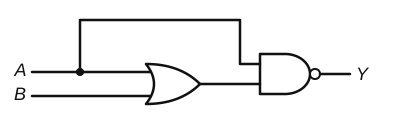
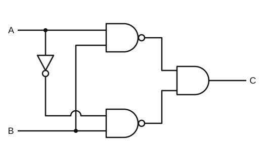
The upper gate is a NOR gate: its output is $\overline{A + B}$.
The lower gate is a NAND gate: its output is $\overline{A \cdot B}$.
The final AND gate gives $$Y = \overline{A + B}\cdot\overline{A \cdot B} = (\bar{A}\bar{B})(\bar{A} + \bar{B}) = \bar{A}\bar{B}$$ since $\bar{A}\bar{B}\bar{A} = \bar{A}\bar{B}$ and $\bar{A}\bar{B}\bar{B} = \bar{A}\bar{B}$.
$Y = \bar{A}\bar{B} = \overline{A + B}$, which is the NOR function.
Solution by Sreeraj P, M.Sc Physics
Q 12-14-004NEETNEET 2025Top questionMedium
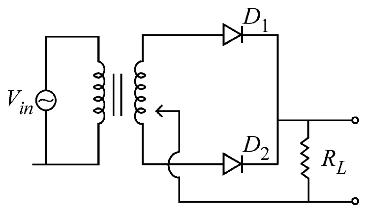
A full wave rectifier circuit with diodes ($D_1$) and ($D_2$) is shown in the figure. If input supply voltage $V_{in} = 220\sin(100\pi t)$ volt, then at $t = 15$ msec
Answer: (B) $D_1$ is reverse biased, $D_2$ is forward biased
At $t = 15$ ms: $100\pi \times 0.015 = 1.5\pi$, and $\sin(1.5\pi) = -1$. The input is at its negative peak, i.e. in the negative half cycle.
In a centre-tap full wave rectifier, $D_1$ conducts during the positive half cycle and $D_2$ during the negative half cycle.
So at $t = 15$ ms, $D_1$ is reverse biased and $D_2$ is forward biased.
Solution by Sreeraj P, M.Sc Physics
Q 12-14-005NEETNEET 2024Top questionEasy
Consider the following statements A and B and identify the correct answer :
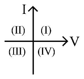
A. For a solar-cell, the I-V characteristics lies in the IV quadrant of the given graph. B. In a reverse biased pn junction diode, the current measured in ($\mu$A), is due to majority charge carriers.
Look at the table: $Y = 1$ exactly when $B = 0$, and $Y = 0$ exactly when $B = 1$, whatever the value of $A$.
So $Y = \bar{B}$.
(Check the other options: $A \cdot B + \bar{A}$ gives $1$ for $A = 0, B = 1$, and $A\cdot\bar{B} + \bar{A}$ also gives $1$ for $A = 0, B = 1$; both disagree with the table.)
Solution by Sreeraj P, M.Sc Physics
Q 12-14-008NEETNEET 2023Top questionEasy
A full wave rectifier circuit consists of two p-n junction diodes, a centre-tapped transformer, capacitor and a load resistance. Which of these components remove the ac ripple from the rectified output?
The diodes rectify (make the output unidirectional), and the transformer supplies the two halves of the input.
The capacitor connected across the load acts as a filter. It charges near each peak and discharges slowly through the load between peaks, smoothing out the ac ripple.
Solution by Sreeraj P, M.Sc Physics
Q 12-14-009NEETNEET 2023Top questionEasy
Given below are two statements:
Statement I : Photovoltaic devices can convert optical radiation into electricity.
Statement II : Zener diode is designed to operate under reverse bias in breakdown region.
In the light of the above statements, choose the most appropriate answer from the options given below :
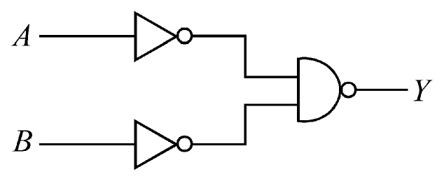
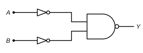
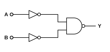
$A$ and $B$ each pass through a NOT gate, and the results go into a NAND gate: $$Y = \overline{\bar{A} \cdot \bar{B}} = A + B$$ (De Morgan's theorem). The circuit is an OR gate.
OR truth table: $Y = 0$ only when $A = B = 0$, otherwise $Y = 1$. This is option (2).
Solution by Sreeraj P, M.Sc Physics
Q 12-14-011NEETNEET 2021Top questionEasy
Consider the following statements (A) and (B) and identify the correct answer.
(A) A zener diode is connected in reverse bias, when used as a voltage regulator.
(B) The potential barrier of p-n junction lies between $0.1$ V to $0.3$ V.
(A) A Zener diode regulates voltage in reverse breakdown, so it is connected in reverse bias. Correct.
(B) The barrier potential is about $0.7$ V for silicon and about $0.3$ V for germanium. It does not in general lie between $0.1$ V and $0.3$ V. Incorrect.
Solution by Sreeraj P, M.Sc Physics
Q 12-14-012NEETNEET 2021Top questionEasy
The electron concentration in an n-type semiconductor is the same as hole concentration in a p-type semiconductor. An external field (electric) is applied across each of them. Compare the currents in them.
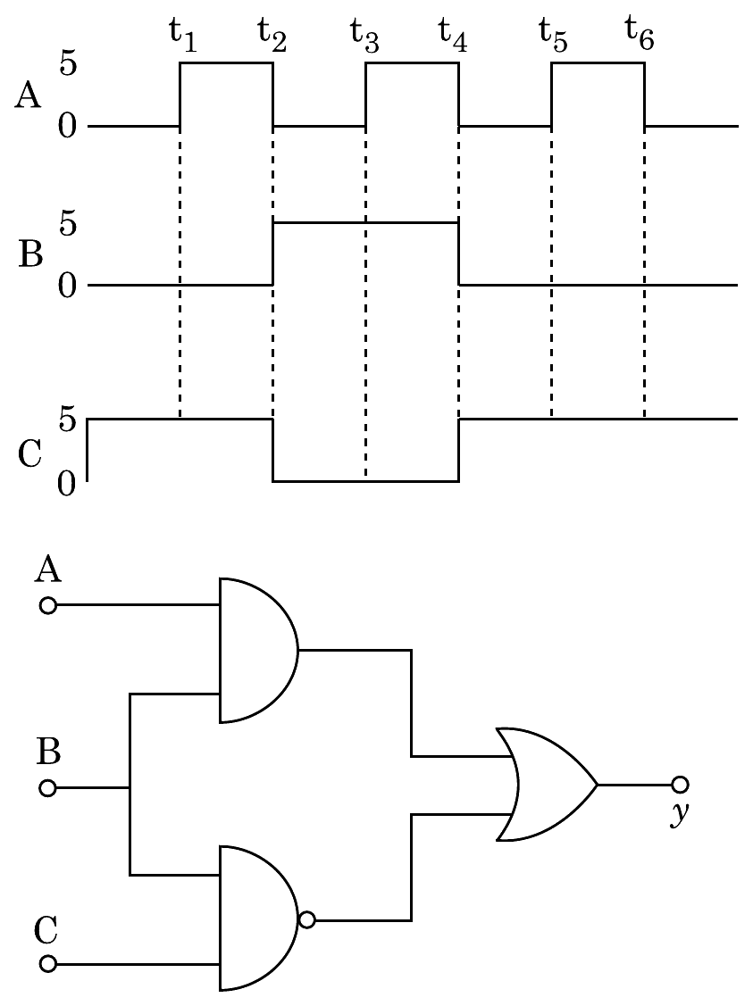
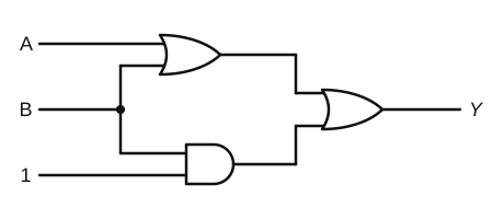
The circuit gives $$y = (A \cdot B) + \overline{(B \cdot C)}$$ (an AND gate on A, B and a NAND gate on B, C, both feeding an OR gate).
From the waveforms, B is high only between $t_2$ and $t_4$, and during exactly that interval C is low. So $B$ and $C$ are never high together: $B \cdot C = 0$ at all times, and the NAND output $\overline{B \cdot C} = 1$ throughout.
An OR gate with one input permanently at 1 gives $y = 1$ at all times: a constant $5$ V, which is option (3).
Solution by Sreeraj P, M.Sc Physics
Q 12-14-014NEETNEET 2020Top questionEasy
The increase in the width of the depletion region in a p-n junction diode is due to :
Answer: (D) The base region must be very thin and lightly doped.
For transistor action, the emitter is heavily doped, the base is very thin and lightly doped, and the collector is moderately doped and large. The emitter junction is forward biased and the collector junction is reverse biased.
A thin, lightly doped base lets most carriers from the emitter cross it to the collector. Only statement (4) is correct.
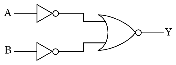
Each input passes through a NOT gate, and the outputs go into a NOR gate: $$Y = \overline{\bar{A} + \bar{B}} = A \cdot B$$ (De Morgan's theorem). The circuit is an AND gate.
AND truth table: $Y = 1$ only when $A = B = 1$. This is option (1).
Solution by Sreeraj P, M.Sc Physics
Q 12-14-017NEETJEE MainEasy
A silicon diode (cut-in voltage $0.7$ V) is connected in forward bias in series with a $1\ \text{k}\Omega$ resistor across a $5$ V battery. The current in the circuit is
The diode takes $0.7$ V, so the resistor has $5 - 0.7 = 4.3$ V across it.
$I = \dfrac{4.3}{1000} = 4.3$ mA.
Solution by Sreeraj P, M.Sc Physics
Q 12-14-018NEETJEE MainMedium
A germanium diode (cut-in $0.3$ V) and a silicon diode (cut-in $0.7$ V) are connected in parallel, both pointing in the forward direction. This pair is connected in series with a $10\ \text{k}\Omega$ resistor across a $12$ V battery. Which diode conducts, and what is the current drawn from the battery?
The Ge diode switches on first and holds the voltage across the parallel pair at $0.3$ V. That is less than the $0.7$ V the Si diode needs, so the Si diode stays off.
$I = \dfrac{12 - 0.3}{10\,000} = 1.17$ mA.
Solution by Sreeraj P, M.Sc Physics
Q 12-14-019NEETJEE MainEasy
Two identical silicon diodes (cut-in $0.7$ V each) are connected in series, both forward biased, with a $2.3\ \text{k}\Omega$ resistor across a $6$ V supply. The current is
Drop across the two diodes $= 1.4$ V, so the resistor has $6 - 1.4 = 4.6$ V.
$I = \dfrac{4.6}{2300} = 2$ mA.
Solution by Sreeraj P, M.Sc Physics
Q 12-14-020NEETJEE MainTop questionMedium
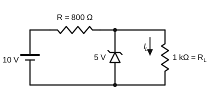
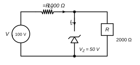
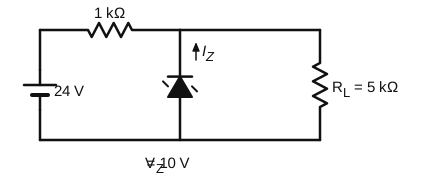
A Zener diode with breakdown voltage $6$ V is used as a voltage regulator. It is connected to a $15$ V supply through a series resistor of $500\ \Omega$, and a load of $1.5\ \text{k}\Omega$ is connected across the Zener. The current through the Zener diode is
The load gets the Zener voltage, $6$ V: $I_L = \dfrac{6}{1500} = 4$ mA.
Current through the series resistor: $I = \dfrac{15 - 6}{500} = 18$ mA.
Zener current $= 18 - 4 = 14$ mA.
Solution by Sreeraj P, M.Sc Physics
Q 12-14-021NEETJEE MainMedium
A $10$ V Zener diode has a maximum power rating of $0.5$ W. It is connected to a $20$ V supply through a series resistor with no load connected. The minimum value of the series resistor that protects the Zener is
The emitted photon carries about the band gap energy: $\lambda = \dfrac{hc}{E_g} = \dfrac{1240}{2.48} = 500$ nm (green light).
Solution by Sreeraj P, M.Sc Physics
Q 12-14-023NEETJEE MainMedium
Three photodiodes $D_1$, $D_2$ and $D_3$ are made of semiconductors with band gaps $2.5$ eV, $2.0$ eV and $1.4$ eV respectively. Light of wavelength $600$ nm falls on each. Which of them can detect it? ($hc = 1240$ eV nm)
Photon energy $= \dfrac{1240}{600} \approx 2.07$ eV.
A photodiode detects light only if the photon energy is at least the band gap. $2.07$ eV exceeds $2.0$ eV and $1.4$ eV but not $2.5$ eV, so only $D_2$ and $D_3$ respond.
Solution by Sreeraj P, M.Sc Physics
Q 12-14-024NEETJEE MainMedium
Pure silicon has an intrinsic carrier concentration of $1.5 \times 10^{16}\ \text{m}^{-3}$. It is doped with $4.5 \times 10^{22}$ donor atoms per m$^3$. The hole concentration in the doped crystal is
An n-type semiconductor has an electron concentration of $10^{21}\ \text{m}^{-3}$ and electron mobility $0.4\ \text{m}^2\,\text{V}^{-1}\text{s}^{-1}$. Neglecting holes, find its electrical conductivity in S m$^{-1}$. ($e = 1.6 \times 10^{-19}$ C)
Answer: (A) decreases, because more electron–hole pairs are produced
Heating gives more valence electrons enough energy to cross the band gap, so the number of free electrons and holes rises sharply. This outweighs the small fall in mobility, so resistance decreases: semiconductors have a negative temperature coefficient of resistance.
Solution by Sreeraj P, M.Sc Physics
Q 12-14-027NEETJEE MainEasy
Silicon is doped with a small amount of phosphorus. The resulting crystal, taken as a whole, is
Phosphorus (valency 5) adds a free electron, making the crystal n-type. But each phosphorus atom that gives up an electron becomes a positive ion, and every atom added was neutral, so the crystal as a whole stays neutral. "n-type" describes the majority carriers, not the net charge.
Solution by Sreeraj P, M.Sc Physics
Q 12-14-028NEETJEE MainEasy
A $60$ Hz AC supply is fed to a full-wave rectifier. The fundamental frequency of the ripple in the output is
A full-wave rectifier gives an output pulse in each half cycle, so there are two pulses per input cycle: $2 \times 60 = 120$ Hz. (A half-wave rectifier would give $60$ Hz.)
Solution by Sreeraj P, M.Sc Physics
Q 12-14-029NEETJEE MainMedium
A bridge rectifier made of four silicon diodes (each dropping $0.7$ V when conducting) is fed an AC voltage of peak value $10$ V. The peak voltage across the load is
In a common-emitter amplifier the current gain is $50$, the input resistance is $1\ \text{k}\Omega$ and the load resistance is $4\ \text{k}\Omega$. The power gain of the amplifier is
Voltage gain $A_v = \beta \dfrac{R_L}{R_i} = 50 \times \dfrac{4}{1} = 200$.
Power gain $= \beta \times A_v = 50 \times 200 = 10^4$.
Solution by Sreeraj P, M.Sc Physics
Q 12-14-032JEE MainHard
An n-p-n transistor in common-emitter mode has $V_{CC} = 10$ V, collector resistor $R_C = 2\ \text{k}\Omega$ and $\beta = 100$. Taking $V_{CE} = 0$ at saturation, find the minimum base current (in $\mu$A) that drives the transistor into saturation.
One NAND gate gives $\overline{A\cdot B}$. A second NAND gate with its two inputs joined acts as a NOT gate and inverts this to $A\cdot B$. So two gates are enough, and one is not.
Solution by Sreeraj P, M.Sc Physics
Q 12-14-035NEETJEE MainMedium
For the input pairs $(A, B) = (0,0), (0,1), (1,0), (1,1)$ in that order, the output of $Y = \overline{A}B + A\overline{B}$ is
$Y$ is $1$ only when exactly one input is $1$ (this is the XOR gate): $(0,0) \to 0$, $(0,1) \to 1$, $(1,0) \to 1$, $(1,1) \to 0$.
Solution by Sreeraj P, M.Sc Physics
Q 12-14-036NEETJEE MainMedium
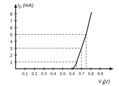
When the forward voltage across a diode is increased from $0.70$ V to $0.75$ V, the current rises from $10$ mA to $20$ mA. The dynamic resistance of the diode in this range is
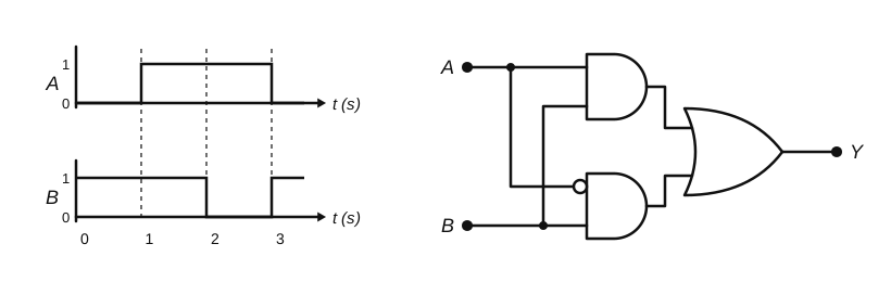
Concept. $Y=AB+\bar AB=B$. So the output simply copies B.
Step 1. Read B. $1$ from $0$ to $2$ s, $0$ from $2$ to $3$ s, $1$ after $3$ s.
Answer. Option B.
Solution by Sreeraj P, M.Sc Physics
Q 12-14-038JEE MainJEE Main 2026 (6 Apr, Shift 1)Medium
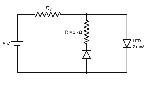
The maximum rated power of the LED is $2$ mW and it is used in the circuit with input voltage of $5$ V as shown in the figure below. The current through resistance $R_S$ is $0.5$ mA.
The minimum value of the resistance of $R_S$, to ensure that the LED is not damaged is ______ k$\Omega$.
Concept. The branch with the reverse-biased diode carries no current, so all $0.5$ mA flows through the LED. Its voltage follows from its power rating.
Step 1. LED voltage. $V=\dfrac{P}{I}=\dfrac{2\times10^{-3}}{0.5\times10^{-3}}=4$ V.
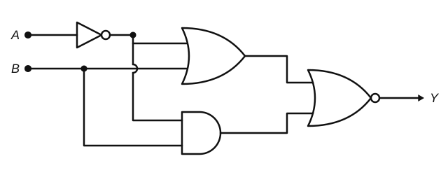
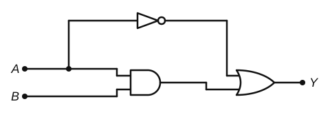
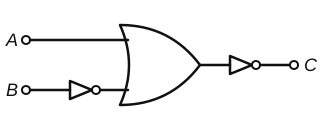
$A$ passes through a NOT gate, giving $\overline{A}$. The OR gate gives $\overline{A} + B$ and the AND gate gives $\overline{A}B$. The final NOR gate gives $$Y = \overline{(\overline{A} + B) + \overline{A}B} = \overline{\overline{A} + B}$$ (since $\overline{A}B$ is already included in $\overline{A} + B$).
With $B = 1$, $\overline{A} + B = 1$ for either value of $A$, so $Y = 0$ in both cases.
Solution by Sreeraj P, M.Sc Physics
Q 12-14-040JEE MainJEE Main 2026 (5 Apr, Shift 1)Medium
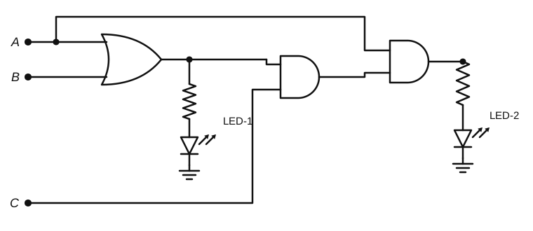
For the given logic circuit, which of the following inputs combination will make both LED-1 and LED-2 to glow?
Step 1. Conditions. Both glow when $A=1$ and $C=1$ (then $A+B=1$ too).
Step 2. Pick. $A=1$, $B=0$, $C=1$.
Answer. Option C.
Solution by Sreeraj P, M.Sc Physics
Q 12-14-041JEE MainJEE Main 2026 (5 Apr, Shift 2)Easy
In a semiconductor $p$-n diode, the doping concentrations on $p$-side and $n$-side are $10^{15}$ atoms/cm$^3$ and $10^{18}$ atoms/cm$^3$, respectively. Which one of the following statements is true?
Answer: (B) The depletion region width is more on p-side compared to that in n-side
Concept. The depletion region holds equal and opposite charge on the two sides. The lightly doped side has fewer ions per volume, so it must be wider.
Answer. Wider on the p-side (Option B).
Solution by Sreeraj P, M.Sc Physics
Q 12-14-042JEE MainJEE Main 2026 (4 Apr, Shift 2)Easy
Given below are two statements: one is labelled as Assertion A and the other is labelled as Reason R
Assertion A : A diode under reverse-biased condition provides very small current which is nearly independent of voltage until a critical limit at which the current increases drastically.
Reason R : Below the critical voltage limit, only majority charge carriers flow which increases drastically above critical voltage.
choose the correct answer from the options given below
Concept. Reverse current is the drift of minority carriers, small and nearly constant, until breakdown. The reason given (majority carriers) is wrong.
Answer. A true, R false (Option C).
Solution by Sreeraj P, M.Sc Physics
Q 12-14-043JEE MainJEE Main 2026 (4 Apr, Shift 2)Easy
A diode has Zener voltage of $10$ V and maximum power dissipation of $0.5$ W, then the minimum resistance to be used in series with this diode for safety when it is connected to a $25$ V power supply is ______ $\Omega$.
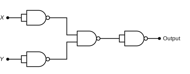
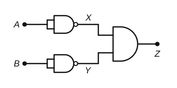
Concept. A NAND gate with its inputs joined is a NOT gate.
Step 1. First stage. $\bar X$ and $\bar Y$.
Step 2. NAND. $\overline{\bar X\bar Y}=X+Y$.
Step 3. Last NAND (NOT). $\overline{X+Y}$.
Answer. NOR gate (Option D).
Solution by Sreeraj P, M.Sc Physics
Q 12-14-046JEE MainJEE Main 2026 (28 Jan, Shift 2)Easy
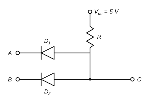
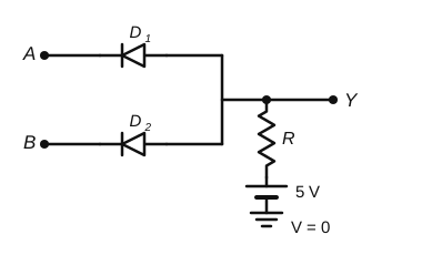
Two p-n junction diodes $D_1$ and $D_2$ are connected as shown in figure. $A$ and $B$ are input signals and $C$ is the output. The given circuit will function as a ______.
Concept. Each diode points from the output C to an input. If any input is at 0 V, its diode conducts and pulls C down to about 0; only when both inputs are high are both diodes off, and R pulls C up to 5 V.
Step 1. Truth table. C $=1$ only for $A=B=1$: AND.
Answer. Option A.
Solution by Sreeraj P, M.Sc Physics
Q 12-14-047JEE MainJEE Main 2026 (28 Jan, Shift 1)Easy
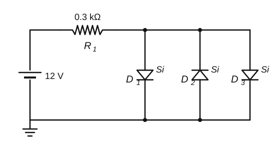
Assuming in forward bias condition there is a voltage drop of 0.7 V across a silicon diode, the current through diode $D_1$ in the circuit is ______ mA .
(Assume all diodes in the given circuit are identical)
Concept. $D_2$ is reverse biased and carries nothing. $D_1$ and $D_3$ are identical and in parallel, so each carries half the current; the drop across the pair is $0.7$ V.
Step 1. Current from the cell. $I=\dfrac{12-0.7}{300}=37.7$ mA.
Step 2. Through $D_1$. $\dfrac{37.7}{2}=18.8$ mA.
Answer. Option B.
Solution by Sreeraj P, M.Sc Physics
Q 12-14-048JEE MainJEE Main 2026 (24 Jan, Shift 2)Medium
Identify the correct truth table of the given logic circuit.
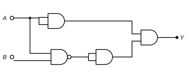
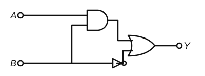
The top AND gate has both inputs connected to $A$: output $= A\cdot A = A$.
The lower gate is a NAND of $A$ and $B$: output $\overline{AB}$. It passes through an AND gate with both inputs tied together, which leaves it unchanged: $\overline{AB}$.
The final AND gate: $Y = A\cdot\overline{AB}$.
$A=0$: $Y = 0$ (for both $B$).
$A=1, B=0$: $\overline{AB} = 1$, $Y = 1$.
$A=1, B=1$: $\overline{AB} = 0$, $Y = 0$.
So $Y = A\overline B$: outputs $0, 0, 1, 0$. This is table (A).
Solution by Sreeraj P, M.Sc Physics
Q 12-14-049JEE MainJEE Main 2026 (24 Jan, Shift 1)Easy
A voltage regulating circuit consisting of Zener diode, having break-down voltage of 10 V and maximum power dissipation of 0.4 W , is operated at 15 V . The approximate value of protective resistance in this circuit is ______ $\Omega$.
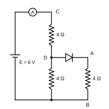
Concept. The diode between D and A points from D to A, so it conducts and acts as a wire. The two $4\ \Omega$ resistors from D to B are then in parallel.
Step 1. Total resistance. $4+2=6\ \Omega$ (A true, E false).
Step 2. Current. $\dfrac66=1$ A (B true).
Step 3. Potentials. $V_{CD}=1\times4=4$ V (D true); $V_{AB}=1\times2=2$ V (C false).
Answer. A, B and D only (Option A).
Solution by Sreeraj P, M.Sc Physics
Q 12-14-052JEE MainJEE Main 2025 (23 Jan, Shift 2)Easy
What is the current through the battery in the circuit shown below?
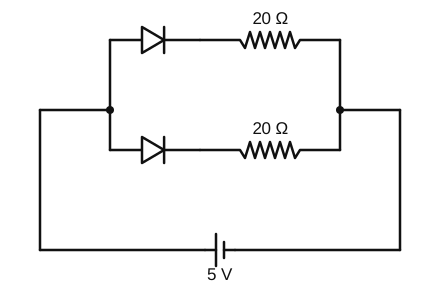
Both diodes point the same way and are forward biased by the cell (treat them as ideal, zero resistance in forward bias).
The two branches, each a diode with $20\ \Omega$, are then in parallel: $$R = \frac{20\times20}{20+20} = 10\ \Omega$$ $$I = \frac{5}{10} = 0.5\ \text{A}$$
Solution by Sreeraj P, M.Sc Physics
Q 12-14-053JEE MainJEE Main 2025 (24 Jan, Shift 1)Medium
Consider the following statements:
A. The junction area of solar cell is made very narrow compared to a photodiode.
B. Solar cells are not connected with any external bias.
C. LED is made of lightly doped p-n junction.
D. Increase of forward current results in continuous increase of LED light intensity.
E. LEDs have to be connected in forward bias for emission of light.
Choose the correct answer from the options given below:
Concept. Solar cells have a large junction area to collect light and need no bias; LEDs are heavily doped and emit only in forward bias, and their light output levels off at high current.
Step 1. Check. A false, B true, C false, D false, E true.
Answer. B, E only (Option A).
Solution by Sreeraj P, M.Sc Physics
Q 12-14-054JEE MainJEE Main 2025 (24 Jan, Shift 2)Easy
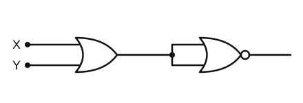
The output of the circuit is low (zero) for:
(A) $X = 0, Y = 0$ (B) $X = 0, Y = 1$ (C) $X = 1, Y = 0$ (D) $X = 1, Y = 1$
Choose the correct answer from the options given below:
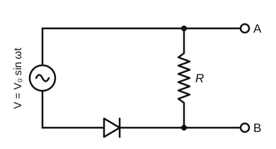
Concept. The diode lets current go round the loop in one direction only: from the source's lower terminal through the diode, up through R from B to A, and back.
Step 1. Conducting half. Current through R flows from B to A, so $V_{AB}=V_A-V_B$ is negative; it follows the negative half-cycle of the source.
Step 2. Other half. The diode blocks; $V_{AB}=0$.
Answer. Negative half-cycles only (Option D).
Solution by Sreeraj P, M.Sc Physics
Q 12-14-057JEE MainJEE Main 2025 (29 Jan, Shift 1)Medium
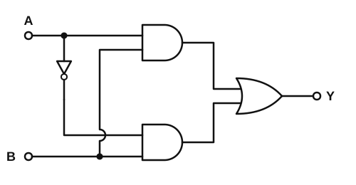
Concept. Write each gate's output: the AND gates give $A\bar B$ and $\bar AB$; the OR gate adds them: $Y=A\bar B+\bar AB$, the XOR function.
Step 1. Table. $Y=1$ only when the inputs differ: $0,1,1,0$.
Answer. Option D.
Solution by Sreeraj P, M.Sc Physics
Q 12-14-059JEE MainJEE Main 2024 (1 Feb, Shift 1)Medium
In the given circuit, the power rating of the Zener diode is $10\ \text{mW}$. The value of the series resistance $R_s$ needed to regulate the unregulated input supply is
Q 12-14-060JEE MainJEE Main 2024 (1 Feb, Shift 2)Easy
The conductivity of a photodiode starts changing only if the wavelength of the incident light is less than $660\ \text{nm}$. The band gap of the photodiode is found to be $\dfrac{X}{8}\ \text{eV}$. The value of $X$ is (Given $h = 6.6\times10^{-34}\ \text{J s}$, $e = 1.6\times10^{-19}\ \text{C}$)
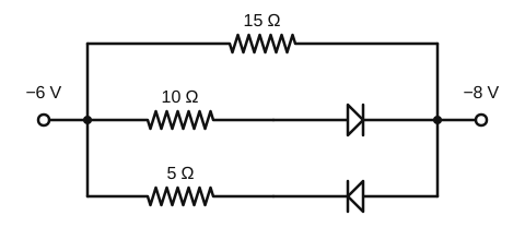
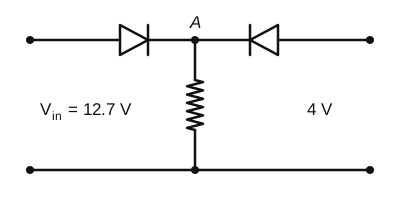
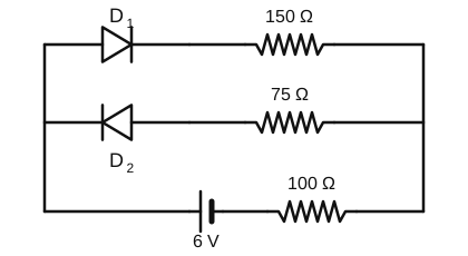
The left terminal ($-6\ \text{V}$) is at the higher potential, so current tends to flow from left to right.
The diode in the $10\ \Omega$ branch points left to right: forward biased, it conducts. The diode in the $5\ \Omega$ branch points right to left: reverse biased, no current. $$R = \frac{15\times10}{15 + 10} = 6\ \Omega$$
Solution by Sreeraj P, M.Sc Physics
Q 12-14-062JEE MainJEE Main 2024 (4 Apr, Shift 2)Easy
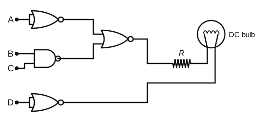
Concept. A bulb between two gate outputs glows only when the outputs differ. Left output: $\overline{\bar A+\overline{BC}}=ABC$. Right output: $\bar D$.
Step 1. Check. A: $0$ and $0$. B: $0$ and $0$. C ($1,0,0,0$): $ABC=0$, $\bar D=1$: different. D: $1$ and $1$.
Answer. Option C.
Solution by Sreeraj P, M.Sc Physics
Q 12-14-064JEE MainJEE Main 2024 (5 Apr, Shift 2)Easy
The output ($Y$) of the logic circuit given below is 0 only when
Q 12-14-066JEE MainJEE Main 2024 (6 Apr, Shift 2)Easy
The acceptor level of a p-type semiconductor is $6\ \text{eV}$. The maximum wavelength of light which can create a hole would be (Given $hc = 1242\ \text{eV nm}$)
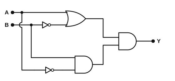
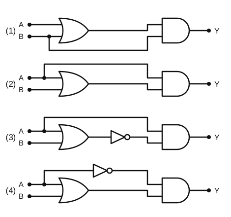
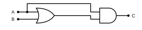
OR gate output: $A + \bar B$. Lower AND gate output: $\bar A B$. $$Y = (A + \bar B)\,\bar AB = A\bar AB + \bar A B\bar B = 0 + 0 = 0$$
Solution by Sreeraj P, M.Sc Physics
Q 12-14-072JEE MainJEE Main 2024 (8 Apr, Shift 2)Medium
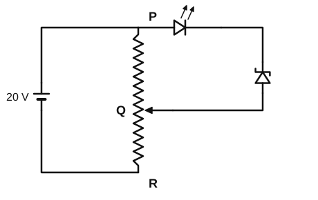
A potential divider circuit is connected with a dc source of $20\ \text{V}$, a light emitting diode of glow-in voltage $1.8\ \text{V}$ and a Zener diode of breakdown voltage $3.2\ \text{V}$. The length (PR) of the resistive wire is $20\ \text{cm}$. The minimum length of PQ to just glow the LED is ______ cm.
Concept. The LED and the reverse-biased Zener are in series across PQ; the LED glows once PQ has $1.8+3.2=5$ V across it. The wire divides $20$ V evenly along its $20$ cm.
Step 1. Potential gradient. $\dfrac{20}{20}=1$ V cm$^{-1}$.
Step 2. Length. $PQ=5$ cm.
Answer. $5$.
Solution by Sreeraj P, M.Sc Physics
Q 12-14-073JEE MainJEE Main 2024 (9 Apr, Shift 1)Easy
A light emitting diode (LED) is fabricated using GaAs semiconducting material whose band gap is $1.42\ \text{eV}$. The wavelength of light emitted from the LED is:
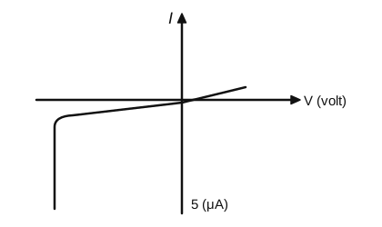
Answer: (B) a zener diode which can be used as a voltage regulator
Concept. An ordinary diode carries a tiny reverse current; a Zener diode carries a tiny reverse current until a definite reverse voltage, where the current rises sharply while the voltage stays almost fixed.
Step 1. Identify. The sharp fall at a large reverse voltage is Zener breakdown: the device is a Zener diode, used as a voltage regulator.
Answer. Option B.
Solution by Sreeraj P, M.Sc Physics
Q 12-14-075JEE MainJEE Main 2024 (9 Apr, Shift 2)Medium
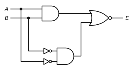
In the truth table of the circuit shown, the values of $X$ and $Y$ are:
$$\begin{array}{c|c|c} A & B & E \\ \hline 0 & 0 & 0 \\ 0 & 1 & X \\ 1 & 0 & Y \\ 1 & 1 & 0 \end{array}$$
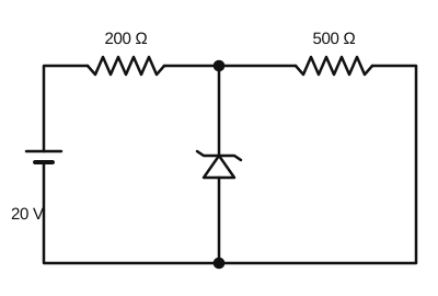
Current through the $200\ \Omega$ resistor: $\dfrac{20 - 10}{200} = 50\ \text{mA}$.
Load current: $\dfrac{10}{500} = 20\ \text{mA}$.
Zener current: $50 - 20 = 30\ \text{mA}$.
Solution by Sreeraj P, M.Sc Physics
Q 12-14-077JEE MainJEE Main 2024 (30 Jan, Shift 2)Medium
In the given circuit, a $15\ \text{V}$ battery is connected in series with a germanium diode $D_1$ and a silicon diode $D_2$ (both forward biased), a $1.5\ \text{k}\Omega$ resistor and a load resistance $R_L = 2.5\ \text{k}\Omega$. The voltage across the load resistance $R_L$ is:
The upper OR gate gives $A + \bar B$ and the lower one gives $\bar A + B$. The NOR gate gives $$Y = \overline{(A + \bar B) + (\bar A + B)} = \overline{(A + \bar A) + (B + \bar B)} = \overline{1} = 0$$ So $Y = 0$ for every input combination.
Solution by Sreeraj P, M.Sc Physics
Q 12-14-080JEE MainJEE Main 2023 (29 Jan, Shift 1)Easy
Which of the following statement is not correct in the case of light emitting diodes?
A. It is a heavily doped p-n junction.
B. It emits light only when it is forward biased.
C. It emits light only when it is reverse biased.
D. The energy of the light emitted is equal to or slightly less than the energy gap of the semiconductor used.
Choose the correct answer from the options given below:
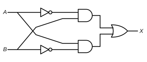
The upper AND gate gives $\bar A B$ and the lower one gives $A\bar B$, so $$X=\bar AB+A\bar B=A\oplus B\ \text{(XOR)}$$ $X=1$ only when the inputs differ: $0,1,1,0$.
Solution by Sreeraj P, M.Sc Physics
Q 12-14-082JEE MainJEE Main 2023 (30 Jan, Shift 1)Medium
The output waveform of the given logical circuit for the following inputs $A$ and $B$ as shown below, is
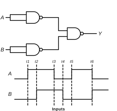
A NAND gate with its inputs joined is a NOT gate, so the first two gates give $\bar A$ and $\bar B$. The last NAND gives $$Y=\overline{\bar A\cdot\bar B}=A+B\quad\text{(OR)}$$ $Y=1$ whenever either input is high: from $t_1$ to $t_4$ ($A$ then $B$ high), $0$ from $t_4$ to $t_5$, and $1$ after $t_5$ ($A$ high until $t_6$, then $B$ high). This is waveform (4).
Solution by Sreeraj P, M.Sc Physics
Q 12-14-083JEE MainJEE Main 2023 (30 Jan, Shift 2)Medium
The output $Y$ for the inputs $A$ and $B$ of circuit is given by the truth table
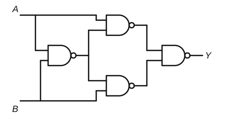
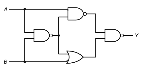
Concept. Call the first NAND output $X=\overline{AB}$. The next two give $\overline{AX}$ and $\overline{BX}$; the last gives $Y=AX+BX=(A+B)\overline{AB}$, the XOR function.
Answer: (B) Both A and R are true but R is NOT the correct explanation of A
Concept. In reverse bias the dark current is tiny, so the light-generated minority carriers change it by a large fraction, making intensity easy to measure. That forward current exceeds reverse current is true but does not explain this.
Answer. Option B.
Solution by Sreeraj P, M.Sc Physics
Q 12-14-087JEE MainJEE Main 2023 (24 Jan, Shift 2)Medium
The logic gate equivalent to the given circuit diagram is
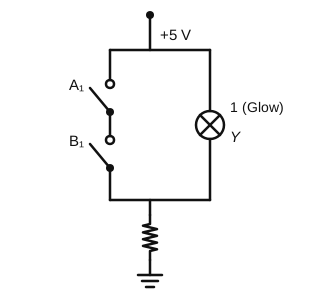
Concept. The switches are in series with each other and the pair is in parallel with the lamp. Closing both shorts the lamp.
Step 1. Table. The lamp is off only when $A_1=B_1=1$: NAND.
Answer. Option B.
Solution by Sreeraj P, M.Sc Physics
Q 12-14-088JEE MainJEE Main 2023 (25 Jan, Shift 1)Easy
Given below are two statements: one is labelled as Assertion A and the other is labelled as Reason R.
Assertion A: Photodiodes are used in forward bias usually for measuring the light intensity.
Reason R: For a $p$-$n$ junction diode, at applied voltage $V$ the current in the forward bias is more than the current in the reverse bias for $|V_z|>\pm V\ge|V_0|$ where $V_0$ is the threshold voltage and $V_z$ is the breakdown voltage.
In the light of the above statements, choose the correct answer from the options given below:
Photodiodes are operated in reverse bias, where the photocurrent is a large fraction of the total current, so A is false. R is a correct statement about diode currents.
Solution by Sreeraj P, M.Sc Physics
Q 12-14-089JEE MainJEE Main 2023 (25 Jan, Shift 2)Easy
Statement I: When a Si sample is doped with Boron, it becomes P-type and when doped by Arsenic it becomes N-type semiconductor such that P-type has excess holes and N-type has excess electrons.
Statement II: When such P-type and N-type semiconductors are fused to make a junction, a current will automatically flow which can be detected with an externally connected ammeter.
In the light of above statements, choose the most appropriate answer from the options given below.
Answer: (D) Statement I is correct but Statement II is incorrect
Concept. Trivalent boron is an acceptor (p-type); pentavalent arsenic is a donor (n-type). When p and n regions meet, carriers diffuse only until the junction field stops them; an unbiased junction carries no steady current.
Step 1. Statement I. Correct.
Step 2. Statement II. Incorrect: an ammeter connected across an unbiased junction reads zero.
Answer. Option D.
Solution by Sreeraj P, M.Sc Physics
Q 12-14-090JEE MainJEE Main 2023 (13 Apr, Shift 2)Medium
The output from a NAND gate having inputs $A$ and $B$ given below will be
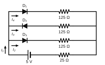
$D_1$ and $D_3$ are forward biased; $D_2$ is reverse biased, so $I_3=0$.
Each conducting branch has $25+125=150\ \Omega$; two in parallel give $75\ \Omega$. With the $25\ \Omega$ in series: $$I_1=\frac{5}{100}=0.05\ \text{A},\qquad I_2=I_4=0.025\ \text{A}$$ So $\dfrac{I_1}{I_2}=2$.
Solution by Sreeraj P, M.Sc Physics
Q 12-14-093JEE MainJEE Main 2023 (11 Apr, Shift 1)Easy
The logic performed by the circuit shown in figure is equivalent to
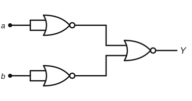
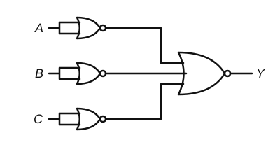
A NOR gate with its inputs joined is a NOT gate, so the first two gates give $\bar a$ and $\bar b$. $$Y=\overline{\bar a+\bar b}=a\cdot b\quad\text{(AND)}$$
Solution by Sreeraj P, M.Sc Physics
Q 12-14-094JEE MainJEE Main 2023 (11 Apr, Shift 2)Medium
The logic operations performed by the given digital circuit is equivalent to
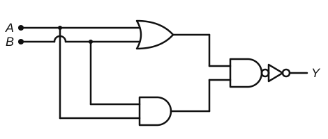
Concept. Follow the gates: NAND of $(A+B)$ and $AB$, then NOT.
Step 1. Output. $(A+B)\cdot AB=AB$.
Answer. AND (Option B).
Solution by Sreeraj P, M.Sc Physics
Q 12-14-095JEE MainJEE Main 2023 (12 Apr, Shift 1)Easy
In an n-p-n common emitter (CE) transistor the collector current changes from $5\ \text{mA}$ to $16\ \text{mA}$ for the change in base current from $100\ \mu\text{A}$ to $200\ \mu\text{A}$, respectively. The current gain of transistor is ______.
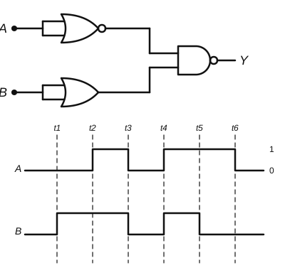
The first gate gives $\bar A$, the second gives $B$, and the NAND gives $$Y=\overline{\bar A\cdot B}=A+\bar B$$ $Y=0$ only when $A=0$ and $B=1$, which happens only between $t_1$ and $t_2$. Everywhere else $Y=1$: waveform (1).
Solution by Sreeraj P, M.Sc Physics
Q 12-14-097JEE MainJEE Main 2023 (13 Apr, Shift 1)Medium
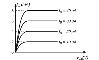
From the given transfer characteristic of a transistor in CE configuration, the value of power gain of this configuration is $10^x$, for $R_B=10\ \text{k}\Omega$ and $R_C=1\ \text{k}\Omega$. The value of $x$ is ______.
In a semiconductor more charge carriers are freed as temperature rises, so the resistivity falls steeply (roughly exponentially) with temperature: graph (3).
Solution by Sreeraj P, M.Sc Physics
Q 12-14-100JEE MainJEE Main 2023 (6 Apr, Shift 2)Medium
Given below are two statements: one is labelled as Assertion A and the other is labelled as Reason R.
Assertion A: Diffusion current in a $p$-$n$ junction is greater than the drift current in magnitude if the junction is forward biased.
Reason R: Diffusion current in a $p$-$n$ junction is from the $n$-side to the $p$-side if the junction is forward biased.
In the light of the above statements, choose the most appropriate answer from the options given below.
Concept. Forward bias lowers the barrier, so diffusion current exceeds drift. Holes diffuse p→n and electrons n→p, so the diffusion current flows from p to n, not n to p.
Answer. A correct, R not correct (Option B).
Solution by Sreeraj P, M.Sc Physics
Q 12-14-101JEE MainJEE Main 2023 (8 Apr, Shift 1)Medium
For the logic circuit shown, the output waveform at $Y$ is
A NAND gate with joined inputs is a NOT gate, so $Y=\overline{\bar A\cdot\bar B}=A+B$ (OR).
From $0$ to $1$ both inputs are $0$, so $Y=0$; from $t=1$ onwards at least one input is $1$, so $Y=1$. Waveform (1).
Solution by Sreeraj P, M.Sc Physics
Q 12-14-102JEE MainJEE Main 2023 (8 Apr, Shift 2)Medium
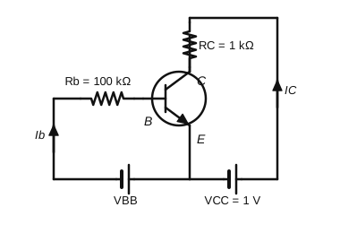
For a given transistor amplifier circuit in CE configuration $V_{CC}=1$ V, $R_C=1\ \text{k}\Omega$, $R_b=100\ \text{k}\Omega$ and $\beta=100$. Value of base current $I_b$ is
Taking the collector–emitter voltage as negligible (transistor driven to saturation), $I_C=\dfrac{V_{CC}}{R_C}=\dfrac{1}{1000}=1$ mA. $$I_b=\frac{I_C}{\beta}=\frac{1\ \text{mA}}{100}=10\ \mu\text{A}$$
Solution by Sreeraj P, M.Sc Physics
Q 12-14-103JEE MainJEE Main 2023 (10 Apr, Shift 1)Medium
A zener diode of power rating $1.6$ W is to be used as voltage regulator. If the zener diode has a breakdown of $8$ V and it has to regulate voltage fluctuating between $3$ V and $10$ V, the value of resistance $R_s$ for safe operation of diode will be
Concept. The Fermi level sits mid-gap in an intrinsic semiconductor, moves towards the conduction band with donors and towards the valence band with acceptors; in metals it lies inside the conduction band.
Answer. A-II, B-III, C-I, D-IV (Option C).
Solution by Sreeraj P, M.Sc Physics
Q 12-14-105JEE MainJEE Main 2023 (1 Feb, Shift 2)Easy
Answer: (A) It works as a voltage regulator in reverse bias and behaves like simple p-n junction diode in forward bias
Concept. In reverse breakdown a Zener holds a fixed voltage over a wide current range; forward biased it behaves like an ordinary diode.
Answer. Option A.
Solution by Sreeraj P, M.Sc Physics
Q 12-14-106JEE MainJEE Main 2022 (24 Jun, Shift 1)Medium
A transistor is used in common-emitter mode in an amplifier circuit. When a signal of $10\ \text{mV}$ is added to the base-emitter voltage, the base current changes by $10\ \mu\text{A}$ and the collector current changes by $1.5\ \text{mA}$. The load resistance is $5\ \text{k}\Omega$. The voltage gain of the transistor will be ______.
Concept. A NOR gate with joined inputs is a NOT gate; then De Morgan.
Step 1. Inputs to last gate. $\bar A$, $\bar B$.
Step 2. NOR. $\overline{\bar A+\bar B}=AB$.
Answer. AND gate (Option A).
Solution by Sreeraj P, M.Sc Physics
Q 12-14-110JEE MainJEE Main 2022 (25 Jun, Shift 2)Medium
In an experiment of CE configuration of an $n$-$p$-$n$ transistor, the transfer characteristics are observed as given in figure. If the input resistance is $200\ \Omega$ and output resistance is $60\ \Omega$, the voltage gain in this experiment will be ______.
Q 12-14-111JEE MainJEE Main 2022 (26 Jun, Shift 1)Medium
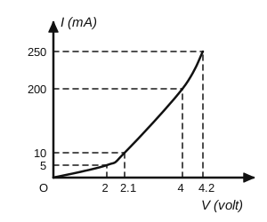
The I–V characteristics of a p–n junction diode in forward bias are shown in the figure. The ratio of dynamic resistance, corresponding to forward bias voltage of $2\ \text{V}$ and $4\ \text{V}$ respectively, is
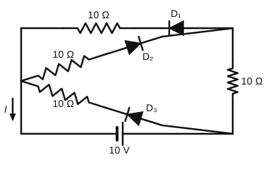
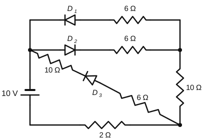
Concept. Follow the current from the positive terminal. A diode conducts if the current would pass from its anode to its cathode; $D_2$ faces the wrong way and stays off, while $D_1$ and $D_3$ conduct.
Step 1. Paths. Through $2\ \Omega$, then two branches back to the negative side: $10\ \Omega+D_1+6\ \Omega$ ($16\ \Omega$) and the diagonal $6\ \Omega+D_3+10\ \Omega$ ($16\ \Omega$).
Step 2. Total. $2+\dfrac{16}{2}=10\ \Omega$.
Step 3. Current. $I=\dfrac{10}{10}=1$ A.
Answer. $1$.
Solution by Sreeraj P, M.Sc Physics
Q 12-14-113JEE MainJEE Main 2022 (26 Jun, Shift 2)Easy
Positive feedback is required by an amplifier to act as an oscillator. The feedback here means
Answer: (B) A portion of the output power is returned back to the input.
Feedback means returning part of the output to the input. With positive feedback, the returned signal is in phase with the input, so the oscillations sustain themselves without any external input.
Solution by Sreeraj P, M.Sc Physics
Q 12-14-114JEE MainJEE Main 2022 (25 Jul, Shift 1)Medium
In the circuit, the logical value of $A = 1$ or $B = 1$ when the potential at $A$ or $B$ is $5\ \text{V}$, and the logical value of $A = 0$ or $B = 0$ when the potential at $A$ or $B$ is $0\ \text{V}$. The truth table of the given circuit will be:
Each diode has its anode at the output node (pulled up to $5\ \text{V}$ through $R$) and its cathode at the input.
If either input is at $0\ \text{V}$, that diode is forward biased and pulls $Y$ down to $0$. Only when both inputs are at $5\ \text{V}$ are both diodes off, and $Y = 5\ \text{V}$.
So $Y = 1$ only for $A = B = 1$: an AND gate, table (1).
Solution by Sreeraj P, M.Sc Physics
Q 12-14-115JEE MainJEE Main 2022 (25 Jul, Shift 1)Easy
The energy band gap of a semiconducting material to produce violet (wavelength $= 4000\ \text{Å}$) LED is ______ eV. (Round off to the nearest integer)
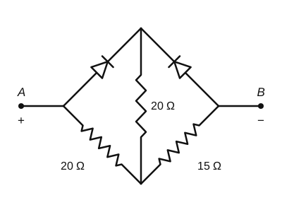
Concept. With A positive, the upper-left diode (pointing from A to the top node) conducts like a wire; the upper-right diode points from B's side towards the top node, so it would need B to be higher: it is off.
Step 1. Redraw. A connects to the top node directly. From A to the bottom node: the vertical $20\ \Omega$ (through the top node) in parallel with the lower-left $20\ \Omega$: $10\ \Omega$.
Step 2. Add. Bottom node to B through $15\ \Omega$: $10+15=25\ \Omega$.
Answer. $25$.
Solution by Sreeraj P, M.Sc Physics
Q 12-14-117JEE MainJEE Main 2022 (26 Jul, Shift 1)Medium
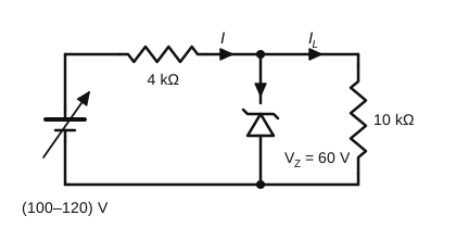
In the circuit shown below, the maximum Zener diode current will be ______ mA.
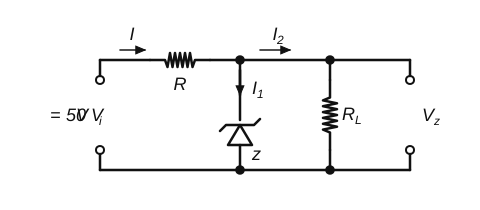
The Zener holds the load at $60\ \text{V}$, so $I_L = \dfrac{60}{10\ \text{k}\Omega} = 6\ \text{mA}$.
The Zener current is largest at the largest input, $120\ \text{V}$: $I = \dfrac{120 - 60}{4\ \text{k}\Omega} = 15\ \text{mA}$. $$I_Z = 15 - 6 = 9\ \text{mA}$$
Solution by Sreeraj P, M.Sc Physics
Q 12-14-118JEE MainJEE Main 2022 (26 Jul, Shift 2)Medium
The typical transfer characteristic of a transistor in CE configuration is shown in figure. A load resistor of $2\ \text{k}\Omega$ is connected in the collector branch of the circuit used. The input resistance of the transistor is $0.50\ \text{k}\Omega$. The voltage gain of the transistor is ______.
As a switch the transistor toggles between cut-off (no collector current: switch OFF) and saturation (maximum current: switch ON). The active region is used for amplification.
Solution by Sreeraj P, M.Sc Physics
Q 12-14-121JEE MainJEE Main 2022 (27 Jun, Shift 2)Easy
The cut-off voltage of the diodes (shown in figure) in forward bias is $0.6$ V. The current through the resister of $40\ \Omega$ is ______ mA.
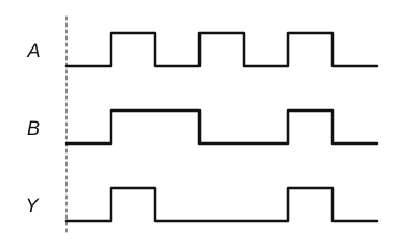
Reading the intervals: $Y = 1$ only where both $A$ and $B$ are $1$ (second and sixth intervals). Where only one input is $1$, or neither, $Y = 0$.
This is an AND gate.
Solution by Sreeraj P, M.Sc Physics
Q 12-14-123JEE MainJEE Main 2022 (27 Jul, Shift 2)Easy
For a constant collector-emitter voltage of $8$ V, the collector current of a transistor reached to the value of $6$ mA from $4$ mA, whereas base current changed from $20\ \mu$A to $25\ \mu$A value. If transistor is in active state, small signal current gain (current amplification factor) will be
Concept. A solar cell drives current into the load with no applied bias: its I–V curve lies in the fourth quadrant, cutting the voltage axis at $V_{oc}$ and the current axis at $-I_{sc}$.
Answer. Option B.
Solution by Sreeraj P, M.Sc Physics
Q 12-14-125JEE MainJEE Main 2021 (27 Jul, Shift 1)Easy
A transistor is connected in common emitter circuit configuration, the collector supply voltage is $10$ V and the voltage drop across a resistor of $1000\ \Omega$ in the collector circuit is $0.6$ V. If the current gain factor $(\beta)$ is $24$, then the base current is ______ $\mu$A. (Round off to the nearest integer)
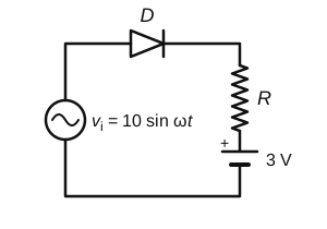
Step 2. Not conducting. For $v_i\lt3$ V, no current and $V_R=0$.
Step 3. Waveform. Positive humps of height 7 V for the part of each cycle with $v_i>3$ V, zero otherwise.
Answer. Option A.
Solution by Sreeraj P, M.Sc Physics
Q 12-14-128JEE MainJEE Main 2021 (31 Aug, Shift 1)Easy
In the following logic circuit the sequence of the inputs $A$, $B$ are $(0, 0)$, $(0, 1)$, $(1, 0)$ and $(1, 1)$. The output $Y$ for this sequence will be:
Q 12-14-129JEE MainJEE Main 2021 (31 Aug, Shift 2)Easy
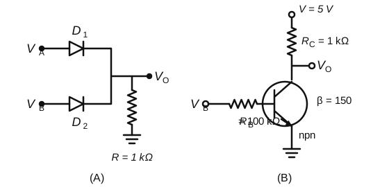
If $V_A$ and $V_B$ are the input voltages (either $5$ V or $0$ V) and $V_0$ is the output voltage then the two gates represented in the following circuits $A$ and $B$ are:
Circuit $A$: if either input is at $5$ V, its diode conducts and $V_0 \approx 5$ V; only when both are $0$ V is $V_0 = 0$. This is an OR gate.
Circuit $B$: with $V_B = 5$ V the transistor saturates and $V_0 \approx 0$; with $V_B = 0$ it is cut off and $V_0 = 5$ V. This is a NOT gate.
Solution by Sreeraj P, M.Sc Physics
Q 12-14-130JEE MainJEE Main 2021 (31 Aug, Shift 2)Easy
Statement I: To get a steady DC output from the pulsating voltage received from a full wave rectifier we can connect a capacitor across the output parallel to the load $R_L$.
Statement II: To get a steady DC output from the pulsating voltage received from a full wave rectifier we can connect an inductor in series with $R_L$.
In the light of the above statements, choose the most appropriate answer from the options given below:
Answer: (B) Both Statement I and Statement II are true
Concept. A capacitor across the load charges at the peaks and discharges slowly between them; an inductor in series opposes changes in current. Both smooth the ripple.
Answer. Both true (Option B).
Solution by Sreeraj P, M.Sc Physics
Q 12-14-131JEE MainJEE Main 2021 (24 Feb, Shift 1)Easy
If an emitter current is changed by 4 mA, the collector current changes by 3.5 mA. The value of $\beta$ will be:
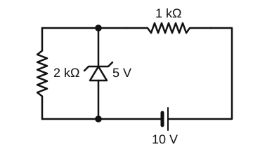
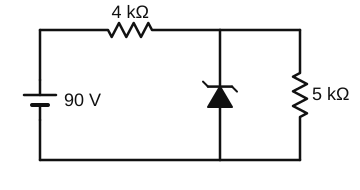
Without the Zener, the 2 kΩ resistor would get $10\times\frac{2}{3} \approx 6.7$ V, more than 5 V, so the Zener breaks down and holds 5 V across the 2 kΩ resistor (they are in parallel). $$I = \frac{5}{2000} = 2.5\times10^{-3}\ \text{A} = 25\times10^{-4}\ \text{A}$$
Solution by Sreeraj P, M.Sc Physics
Q 12-14-133JEE MainJEE Main 2021 (24 Feb, Shift 1)Easy
An audio signal $v_m = 20\sin2\pi(1500t)$ amplitude modulates a carrier $v_c = 80\sin2\pi(100000t)$. The value of percent modulation is ______.
Answer: (D) heavily doped and have narrow depletion layer.
Concept. Zener breakdown needs a very strong field across a thin junction: heavy doping on both sides gives a narrow depletion layer.
Answer. Option D.
Solution by Sreeraj P, M.Sc Physics
Q 12-14-136JEE MainJEE Main 2021 (24 Feb, Shift 2)Easy
Given below are two statements:
Statement I: $p$-$n$ junction diodes can be used to function as a transistor, simply by connecting two diodes, back to back, which acts as the base terminal.
Statement II: In the study of transistors, the amplification factor $\beta$ indicates ratio of the collector current to the base current.
In the light of the above statements, choose the correct answer from the options given below.
Answer: (C) Statement I is false but Statement II is true
Two separate diodes joined back to back do not make a transistor: the base of a transistor must be very thin and lightly doped so that carriers cross it to the collector. Statement I is false.
$\beta = I_C/I_B$ is the current amplification factor. Statement II is true.
Solution by Sreeraj P, M.Sc Physics
Q 12-14-137JEE MainJEE Main 2021 (24 Feb, Shift 2)Easy
A signal of 0.1 kW is transmitted in a cable. The attenuation of cable is $-5$ dB per km and cable length is 20 km. The power received at the receiver is $10^{-x}$ W. The value of $x$ is ______. [Gain in dB $= 10\log_{10}\left(\dfrac{P_o}{P_i}\right)$]
Total gain $= -5\times20 = -100$ dB: $$10\log_{10}\frac{P_o}{P_i} = -100 \Rightarrow \frac{P_o}{P_i} = 10^{-10}$$ $P_o = 100\times10^{-10} = 10^{-8}$ W, so $x = 8$.
Solution by Sreeraj P, M.Sc Physics
Q 12-14-138JEE MainJEE Main 2021 (25 Feb, Shift 1)Medium
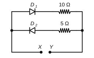
A 5 V battery is connected across the points $X$ and $Y$. Assume $D_1$ and $D_2$ to be normal silicon diodes. Find the current supplied by the battery if the $+ve$ terminal of the battery is connected to point $X$.
With $X$ positive, current tends to flow from the left wire to the right wire through the branches. $D_1$ points from left to right, so it is forward biased; $D_2$ points the other way and is reverse biased (no current).
Taking 0.7 V across the forward-biased silicon diode: $$I = \frac{5 - 0.7}{10} = 0.43\ \text{A}$$
Solution by Sreeraj P, M.Sc Physics
Q 12-14-139JEE MainJEE Main 2021 (25 Feb, Shift 1)Easy
Given below are two statements:
Statement I: A speech signal of 2 kHz is used to modulate a carrier signal of 1 MHz. The bandwidth requirement for the signal is 4 kHz.
Statement II: The side band frequencies are 1002 kHz and 998 kHz.
In the light of the above statements, choose the correct answer from the options given below:
Answer: (B) Both Statement I and Statement II are true
Side bands are at $f_c \pm f_m = 1000 \pm 2$ kHz, i.e. 1002 kHz and 998 kHz. The bandwidth is $2f_m = 4$ kHz. Both statements are true.
Solution by Sreeraj P, M.Sc Physics
Q 12-14-140JEE MainJEE Main 2021 (18 Mar, Shift 2)Easy
The correct relation between $\alpha$ (ratio of collector current to emitter current) and $\beta$ (ratio of collector current to base current) of a transistor is:
Q 12-14-144JEE MainJEE Main 2021 (20 Jul, Shift 1)Easy
A carrier wave $V_C(t) = 160\sin(2\pi\times10^6t)$ volts is made to vary between $V_{max} = 200$ V and $V_{min} = 120$ V by a message signal $V_m(t) = A_m\sin(2\pi\times10^3t)$ volts. The peak voltage $A_m$ of the modulating signal is ______ V.
$V_{max} = A_c + A_m$ and $V_{min} = A_c - A_m$, so $A_m = \dfrac{200 - 120}{2} = 40$ V (and $A_c = 160$ V, as given).
Solution by Sreeraj P, M.Sc Physics
Q 12-14-145JEE MainJEE Main 2021 (20 Jul, Shift 2)Medium
A zener diode having zener voltage 8 V and power dissipation rating of 0.5 W is connected across a potential divider arranged with maximum potential drop across zener diode is as shown in the diagram. The value of protective resistance $R_p$ is ______ $\Omega$.
Q 12-14-147JEE MainJEE Main 2021 (22 Jul, Shift 1)Easy
Consider a situation in which reverse biased current of a particular P-N junction increases when it is exposed to a light of wavelength $\le 621$ nm. During this process, enhancement in carrier concentration takes place due to generation of hole-electron pairs. The value of band gap is nearly.
Q 12-14-148JEE MainJEE Main 2021 (22 Jul, Shift 1)Medium
What should be the height of transmitting antenna and the population covered if the television telecast is to cover a radius of 150 km? The average population density around the tower is $2000\ \text{km}^{-2}$ and the value of $R_e = 6.5\times10^6$ m.
Answer: (A) Height = 1731 m, Population Covered = $1413\times10^5$
$d = \sqrt{2Rh} \Rightarrow h = \dfrac{d^2}{2R} = \dfrac{(1.5\times10^5)^2}{2\times6.5\times10^6} \approx 1731$ m.
Area covered $= \pi d^2 = 3.14\times150^2 \approx 7.07\times10^4\ \text{km}^2$. Population $= 7.07\times10^4\times2000 \approx 1.413\times10^8 = 1413\times10^5$.
Solution by Sreeraj P, M.Sc Physics
Q 12-14-149JEE MainJEE Main 2021 (22 Jul, Shift 1)Medium
In a given circuit diagram, a 5 V zener diode along with a series resistance is connected across a 50 V power supply. The minimum value of the resistance required, if the maximum zener current is 90 mA will be ______ $\Omega$.
The Zener current is largest when the load draws no current, so then all the current through $R$ passes through the Zener: $$I_{max} = \frac{50 - 5}{R} \le 90\ \text{mA} \Rightarrow R \ge \frac{45}{0.09} = 500\ \Omega$$
Solution by Sreeraj P, M.Sc Physics
Q 12-14-150JEE MainJEE Main 2021 (26 Feb, Shift 1)Easy
LED is constructed from $Ga-As-P$ semiconducting material. The energy gap of this LED is $1.9$ eV. Calculate the wavelength of light emitted and its colour. $h = 6.63\times10^{-34}$ J s and $c = 3\times10^8$ m s$^{-1}$
Step 1. Value. $\dfrac{1243}{1.9}=654$ nm, in the red.
Answer. Option A.
Solution by Sreeraj P, M.Sc Physics
Q 12-14-151JEE MainJEE Main 2021 (26 Feb, Shift 1)Easy
The circuit contains two diodes each with a forward resistance of $50\ \Omega$ and with infinite reverse resistance. If the battery voltage is $6$ V, the current through the $120\ \Omega$ resistance is ______ mA
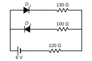
Concept. Decide which diode conducts. $D_2$ is reverse biased (open); $D_1$ conducts with its forward resistance of $50\ \Omega$, so the circuit is one series loop.
Step 1. Total resistance. $120+50+130=300\ \Omega$.
Step 2. Current. $I=\dfrac{6}{300}=0.02$ A $=20$ mA.
Answer. $20$.
Solution by Sreeraj P, M.Sc Physics
Q 12-14-152JEE MainJEE Main 2021 (26 Feb, Shift 2)Medium
Draw the output signal $Y$ in the given combination of gates.
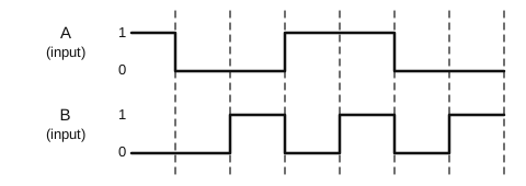
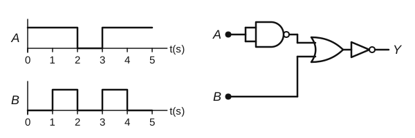
The first gate is a NAND with both inputs tied to $A$, so its output is $\bar{A}$. This goes into an OR gate with $B$, followed by a NOT gate: $$Y = \overline{\bar{A} + B} = A\cdot\bar{B}$$ So $Y = 1$ only when $A = 1$ and $B = 0$.
From the waveforms: $0$–$1$ s ($A=1, B=0$): $Y = 1$; $1$–$2$ s ($B=1$): $Y = 0$; $2$–$3$ s ($A=0$): $Y = 0$; $3$–$4$ s ($B=1$): $Y = 0$; $4$–$5$ s ($A=1, B=0$): $Y = 1$.
The output is high from $0$ to $1$ s and from $4$ to $5$ s.
Solution by Sreeraj P, M.Sc Physics
Q 12-14-153JEE MainJEE Main 2021 (26 Feb, Shift 2)Medium
The zener diode has a $V_z = 30$ V. The current passing through the diode for the following circuit is ______ mA.
Q 12-14-154JEE MainJEE Main 2021 (25 Jul, Shift 2)Easy
In a semiconductor, the number density of intrinsic charge carriers at $27^\circ$C is $1.5\times10^{16}$ m$^{-3}$. If the semiconductor is doped with an impurity atom, the hole density increases to $4.5\times10^{22}$ m$^{-3}$. The electron density in the doped semiconductor is ______ $\times10^9$ m$^{-3}$
Answer: (B) Statement I is true but Statement II is false.
Concept. A pentavalent dopant gives a spare electron, so $n_e$ rises. But each donor atom that gives up an electron becomes a positive ion: the crystal stays neutral.
Answer. Statement I true, II false (Option B).
Solution by Sreeraj P, M.Sc Physics
Q 12-14-157JEE MainJEE Main 2021 (26 Aug, Shift 2)Medium
Four NOR gates are connected as shown in figure. The truth table for the given figure is:
Let $C = \overline{A + B}$ be the output of the first NOR gate. The second and third gates give $\overline{A + C}$ and $\overline{B + C}$, and the last gate gives $$Y = \overline{\overline{A + C} + \overline{B + C}} = (A + C)(B + C) = AB + C = AB + \bar{A}\bar{B}$$ This is XNOR: $Y = 1$ for $(0,0)$ and $(1,1)$, and $Y = 0$ for $(0,1)$ and $(1,0)$.
Solution by Sreeraj P, M.Sc Physics
Q 12-14-158JEE MainJEE Main 2021 (26 Aug, Shift 2)Medium
For the given circuit, the power across zener diode is ______ mW.
Amplification needs the output current to follow the input linearly, which happens only in the active region (emitter-base forward biased, collector-base reverse biased). Cut-off and saturation are used for switching.
Solution by Sreeraj P, M.Sc Physics
Q 12-14-160JEE MainJEE Main 2021 (27 Aug, Shift 1)Medium
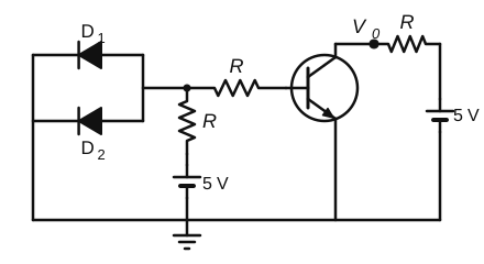
A circuit is arranged as shown in figure. The output voltage $V_0$ is equal to ______ V.
The diodes $D_1$ and $D_2$ are connected from the base-side junction to ground. The $5$ V cell would raise that junction above ground, so the diodes conduct and (being ideal) clamp it at $0$ V.
So the base of the transistor is at $0$ V, the same as the emitter: $V_{BE} = 0$ and the transistor is cut off.
No collector current flows, so there is no drop across the collector resistor $R$, and $V_0 = 5$ V.
Solution by Sreeraj P, M.Sc Physics
Q 12-14-161JEE MainJEE Main 2021 (27 Aug, Shift 2)Easy
For a transistor $\alpha$ and $\beta$ are given as $\alpha = \frac{I_C}{I_E}$ and $\beta = \frac{I_C}{I_B}$. Then the correct relation between $\alpha$ and $\beta$ will be:
Q 12-14-162JEE MainJEE Main 2021 (27 Aug, Shift 2)Medium
A zener diode of power rating $2$ W is to be used as a voltage regulator. If the zener diode has a breakdown of $10$ V and it has to regulate voltage fluctuated between $6$ V and $14$ V, the value of $R_s$ for safe operation should be ______ $\Omega$.
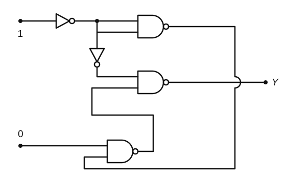
Concept. Trace the fixed inputs first; a NAND gate gives 1 if any input is 0.
Step 1. Top. $1\to$ NOT $\to0$; NAND with both inputs $0$ gives $1$. The second NOT turns the $0$ back into $1$.
Step 2. Bottom NAND. One input is $0$, so its output is $1$ whatever the feedback.
Step 3. Middle NAND. Inputs $1$ (from the NOT) and $1$ (from the bottom gate): $Y=0$, and it stays there.
Answer. $0$ (Option A).
Solution by Sreeraj P, M.Sc Physics
Q 12-14-164JEE MainJEE Main 2020 (9 Jan, Shift 1)Medium
Both the diodes used in the circuit shown are assumed to be ideal and have negligible resistance when these are forward biased. Built in potential in each diode is $0.7$ V. For the input voltages shown in the figure, the voltage (in volts) at point A is ______.
The current $i$ enters the network at the left node. Both diodes point against this flow (the one in the upper-left arm and the one in the lower-right arm), so they are reverse biased and those two arms carry no current.
The only path left is: left node $\to 10\ \Omega \to$ bottom node $\to 5\ \Omega$ (middle) $\to$ top node $\to 10\ \Omega \to$ right node.
Q 12-14-166JEE MainJEE Main 2020 (9 Jan, Shift 2)Medium
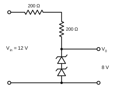
The circuit shown below is working as an $8$ V dc regulated voltage source. When $12$ V is used as an input, the power dissipated (in mW) in each diode is (considering both zener diodes are identical)
Concept. An operation is reversible if the inputs can be recovered from the output. A two-input gate loses information (several input pairs give the same output); a NOT gate does not.
Step 1. Pick. The NOR gate with its inputs joined is a NOT gate: reversible.
Answer. Option D.
Solution by Sreeraj P, M.Sc Physics
Q 12-14-168JEE MainJEE Main 2020 (7 Jan, Shift 2)Medium
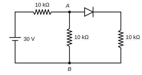
In the figure, the potential difference between A and B is:
The positive (longer) plate of the cell drives current from A through the diode in its forward direction, so the ideal diode conducts and acts as a plain wire.
Then the two $10\ \text{k}\Omega$ resistors between A and B are in parallel: $5\ \text{k}\Omega$. This is in series with the first $10\ \text{k}\Omega$: $$I = \frac{30}{10 + 5}\ \text{mA} = 2\ \text{mA}$$ $$V_{AB} = 2\ \text{mA}\times5\ \text{k}\Omega = 10\ \text{V}$$
Solution by Sreeraj P, M.Sc Physics
Q 12-14-170JEE MainJEE Main 2020 (2 Sep, Shift 2)Medium
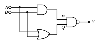
In the following digital circuit, what will be the output $Z$, when the input $(A, B)$ are $(1, 0)$, $(0, 0)$, $(1, 1)$, $(0, 1)$?
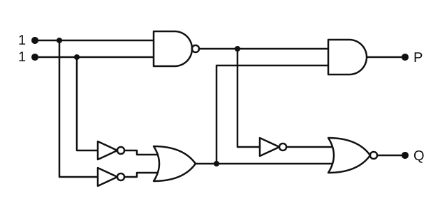
The first gates give $P = \overline{AB}$ (NAND) and $Q = A + B$ (OR). The AND gate gives $P\cdot Q = A \oplus B$. The output NOR gate gives $Z = \overline{P + A\oplus B}$.
$(1,0)$: $P = 1 \Rightarrow Z = 0$. $(0,0)$: $P = 1 \Rightarrow Z = 0$. $(1,1)$: $P = 0$, $A\oplus B = 0 \Rightarrow Z = 1$. $(0,1)$: $P = 1 \Rightarrow Z = 0$.
Output: $0, 0, 1, 0$.
Solution by Sreeraj P, M.Sc Physics
Q 12-14-171JEE MainJEE Main 2020 (3 Sep, Shift 1)Easy
When a diode is forward biased, it has a voltage drop of $0.5\ \text{V}$. The safe limit of current through the diode is $10\ \text{mA}$. If a battery of emf $1.5\ \text{V}$ is used in the circuit, the value of minimum resistance to be connected in series with the diode so that the current does not exceed the safe limit is:
Q 12-14-172JEE MainJEE Main 2020 (3 Sep, Shift 2)Easy
If a semiconductor photo diode can detect a photon with a maximum wavelength of $400\ \text{nm}$, then its band gap energy is: (Planck's constant $h = 6.63\times10^{-34}\ \text{J s}$, speed of light $c = 3\times10^{8}\ \text{m s}^{-1}$)
Q 12-14-173JEE MainJEE Main 2020 (4 Sep, Shift 1)Medium
Take the breakdown voltage of the zener diode used in the given circuit as $6\ \text{V}$. For the input voltage shown in the figure below, the time variation of the output voltage is: (Graphs drawn are schematic and not to the scale)
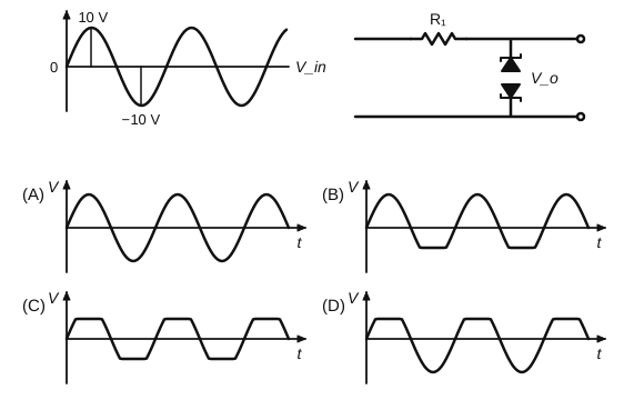
Concept. Back-to-back Zeners: in each half-cycle one is in breakdown ($6$ V) and the other is forward biased ($\approx0$–$0.7$ V), so the output cannot exceed about $\pm6$ V.
Step 1. Output. It follows the input up to about $\pm6$ V and is flat beyond: both halves clipped.
Answer. Option C.
Solution by Sreeraj P, M.Sc Physics
Q 12-14-174JEE MainJEE Main 2020 (4 Sep, Shift 2)Medium
Identify the operation performed by the circuit given below:
Answer: (D) increases initially and saturates finally
Concept. In reverse bias, light makes electron–hole pairs that the junction field sweeps across. Raising the bias collects them more completely until all are collected.
Step 1. Behaviour. The photocurrent rises at first and then saturates.
Answer. Option D.
Solution by Sreeraj P, M.Sc Physics
Q 12-14-176JEE MainJEE Main 2019 (9 Jan, Shift 2)Medium
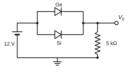
Ge and Si diodes start conducting at $0.3\ \text{V}$ and $0.7\ \text{V}$ respectively. In the following figure if the Ge diode connections are reversed, the value of $V_0$ changes by: (assume that the Ge diode has large breakdown voltage)
Concept. Parallel diodes: the one that turns on first (lower cut-in) fixes the voltage across both.
Step 1. Ge forward. Ge conducts at $0.3$ V: $V_0=12-0.3=11.7$ V.
Step 2. Ge reversed. Only Si conducts: $V_0=12-0.7=11.3$ V.
Step 3. Change. $0.4$ V.
Answer. Option B.
Solution by Sreeraj P, M.Sc Physics
Q 12-14-177JEE MainJEE Main 2019 (10 Jan, Shift 1)Medium
In a logic circuit, input $x$ passes through a NOT gate, and its output and input $y$ are fed to an OR gate whose output is $P$. Input $x$ and the output of a NOT gate fed by $y$ are the inputs of a NAND gate whose output is $Q$. $P$ and $Q$ are the inputs of a NOR gate whose output is $R$.
Q 12-14-178JEE MainJEE Main 2019 (10 Jan, Shift 2)Medium
A $120\ \text{V}$ source is connected through a $5\ \text{k}\Omega$ series resistor to a Zener diode of breakdown voltage $50\ \text{V}$ (reverse biased). A $10\ \text{k}\Omega$ load resistor is connected across the Zener diode. The current through the Zener diode is
Q 12-14-179JEE MainJEE Main 2019 (10 Apr, Shift 1)Medium
An NPN transistor operates as a common emitter amplifier, with a power gain of $60\ \text{dB}$. The input circuit resistance is $100\ \Omega$ and the output load resistance is $10\ \text{k}\Omega$. The common emitter current gain $\beta$ is:
$60\ \text{dB}$ means a power gain of $10^6$. For a CE amplifier $$\text{Power gain} = \beta^2\frac{R_L}{R_{in}} = \beta^2\times\frac{10^4}{100} = 100\,\beta^2$$ So $\beta^2 = 10^4$ and $\beta = 10^2$.
Solution by Sreeraj P, M.Sc Physics
Q 12-14-180JEE MainJEE Main 2019 (10 Apr, Shift 2)Medium
A voltage regulator circuit uses a Zener diode of breakdown voltage $6\ \text{V}$ connected across a load resistance $R_L = 4\ \text{k}\Omega$. A series resistance $R_i = 1\ \text{k}\Omega$ connects this combination to a battery of voltage $V_B$. If $V_B$ varies from $8\ \text{V}$ to $16\ \text{V}$, what are the minimum and maximum values of the current through the Zener diode?
Concept. The load current stays $\dfrac{6}{4\ \text{k}}=1.5$ mA; the Zener takes whatever extra the series resistor passes.
Step 1. At 8 V. $I_s=\dfrac{2}{1\ \text{k}}=2$ mA, $I_z=0.5$ mA.
Step 2. At 16 V. $I_s=10$ mA, $I_z=8.5$ mA.
Answer. Option C.
Solution by Sreeraj P, M.Sc Physics
Q 12-14-181JEE MainJEE Main 2019 (9 Jan, Shift 1)Easy
Mobility of electrons in a semiconductor is defined as the ratio of their drift velocity to the applied electric field. If, for an N-type semiconductor, the density of electrons is $10^{19}\ \text{m}^{-3}$ and their mobility is $1.6\ \text{m}^2\text{V}^{-1}\text{s}^{-1}$, then the resistivity of the semiconductor (since it is an N-type semiconductor contribution of holes is ignored) is close to
Q 12-14-183JEE MainJEE Main 2019 (8 Apr, Shift 2)Easy
A common emitter amplifier circuit, built using an NPN transistor, has its base connected through $R_B$ to a supply $V_B$ and its collector connected through $R_C$ to $V_{CC}$. Its dc current gain is $250$, $R_C = 1\ \text{k}\Omega$ and $V_{CC} = 10\ \text{V}$. The minimum base current for $V_{CE}$ to reach saturation is
At saturation $V_{CE} \approx 0$, so the collector current is limited by $R_C$: $$I_C = \frac{V_{CC}}{R_C} = \frac{10}{1000} = 10\ \text{mA}$$ $$I_B = \frac{I_C}{\beta} = \frac{10\ \text{mA}}{250} = 40\ \mu\text{A}$$
Solution by Sreeraj P, M.Sc Physics
Q 12-14-185JEE MainJEE Main 2019 (9 Apr, Shift 2)Easy
The logic gate equivalent to the given logic circuit is
The inputs are inverted and then fed to a NAND gate: $$Y = \overline{\bar A\cdot\bar B} = \bar{\bar A} + \bar{\bar B} = A + B$$ (De Morgan's theorem). This is an OR gate.
Solution by Sreeraj P, M.Sc Physics
Q 12-14-186JEE MainJEE Main 2019 (11 Jan, Shift 1)Medium
In the given circuit the current through Zener Diode is close to:
Concept. First check whether the Zener breaks down: remove it and find the voltage across its terminals.
Step 1. Without the Zener. The two $1500\ \Omega$ resistors in parallel give $750\ \Omega$; $V=12\times\dfrac{750}{500+750}=7.2$ V.
Step 2. Compare. $7.2$ V $\lt10$ V: the Zener does not break down, so no current flows through it.
Answer. $0$ mA (Option A).
Solution by Sreeraj P, M.Sc Physics
Q 12-14-187JEE MainJEE Main 2019 (11 Jan, Shift 2)Medium
The circuit shown below contains two ideal diodes, each with a forward resistance of $50\ \Omega$. If the battery voltage is $6$ V, the current through the $100\ \Omega$ resistance (in amperes) is:
The cell's positive terminal is on the left, so current goes up the left wire and through the parallel branches from left to right. $D_1$ (pointing right) is forward biased; $D_2$ is reverse biased and carries no current. $$I = \frac{6}{100 + 50 + 150} = 0.02\ \text{A}$$
Solution by Sreeraj P, M.Sc Physics
Q 12-14-188JEE MainJEE Main 2019 (12 Jan, Shift 1)Medium
Q 12-14-189JEE MainJEE Main 2019 (12 Jan, Shift 2)Medium
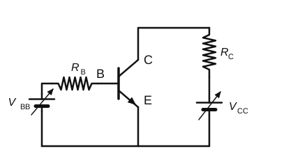
In the figure, given that $V_{BB}$ supply can vary from $0$ to $5.0$ V, $V_{CC} = 5$ V, $\beta_{dc} = 200$, $R_B = 100$ kΩ, $R_C = 1$ kΩ and $V_{BE} = 1.0$ V. The minimum base current and the input voltage at which the transistor will go to saturation, will be, respectively:
Q 12-14-191JEE MainJEE Main 2019 (12 Apr, Shift 1)Medium
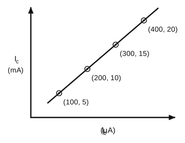
The transfer characteristic curve of a transistor, having input and output resistance $100\ \Omega$ and $100$ kΩ respectively, is shown in the figure. The voltage and power gain, are respectively:
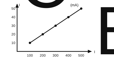
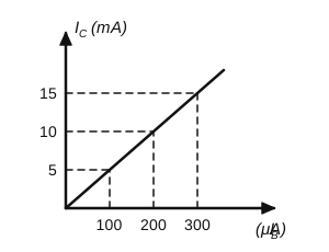
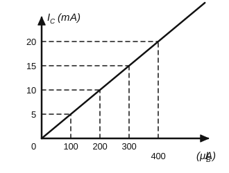
Current gain from the slope: $$\beta = \frac{\Delta I_c}{\Delta I_b} = \frac{5\ \text{mA}}{100\ \mu\text{A}} = 50$$ $$A_V = \beta\frac{R_{\text{out}}}{R_{\text{in}}} = 50\times\frac{10^5}{100} = 5\times10^4,\qquad A_P = \beta A_V = 2.5\times10^6$$
Solution by Sreeraj P, M.Sc Physics
Q 12-14-192JEE MainJEE Main 2019 (12 Apr, Shift 2)Easy
Figure shows a DC voltage regulator circuit, with a Zener diode of breakdown voltage $= 6$ V. If the unregulated input voltage varies between $10$ V to $16$ V, then what is the maximum Zener current?
The Zener current is largest at the largest input, $16$ V: $$I_s = \frac{16 - 6}{2\ \text{k}\Omega} = 5\ \text{mA},\qquad I_L = \frac{6}{4\ \text{k}\Omega} = 1.5\ \text{mA}$$ $$I_Z = 5 - 1.5 = 3.5\ \text{mA}$$
Solution by Sreeraj P, M.Sc Physics
Q 12-14-193JEE MainJEE Main 2019 (12 Apr, Shift 2)Easy
In a CE transistor amplifier, the audio signal voltage across the collector resistance of $2$ kΩ is $2$ V. If the base resistance is $1$ kΩ and the current amplification of the transistor is $100$, then the input signal voltage is
Q 12-14-194JEE MainJEE Main 2018 (15 Apr, Shift 1)Easy
In a common emitter configuration with suitable bias, it is given that $R_L$ is the load resistance and $R_{BE}$ is small-signal dynamic resistance (input side). Then, voltage gain, current gain and power gain are given, respectively, by: ($\beta$ is current gain, $I_B$, $I_C$ and $I_E$ are respectively base, collector, and emitter currents.)
Power gain: $A_P = A_V\times\beta = \beta^2\dfrac{R_L}{R_{BE}}$.
This is option (1).
Solution by Sreeraj P, M.Sc Physics
Q 12-14-195JEE MainJEE Main 2018 (15 Apr, Shift 1)Easy
The number of amplitude-modulated broadcast stations that can be accommodated in a $300\ \text{kHz}$ bandwidth for the highest modulating frequency $15\ \text{kHz}$ will be:
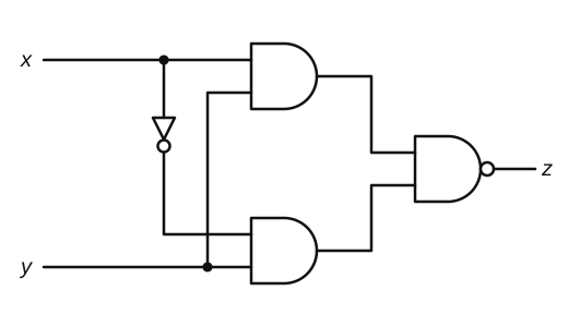
Lower AND gate: inputs $\bar x$ (through the NOT gate) and $y$, output $\bar xy$.
NAND gate: $z = \overline{(xy)(\bar xy)}$.
Since $x\bar x = 0$, the product $(xy)(\bar xy)$ is always $0$, so $$z = \bar 0 = 1$$ for every input. The output column is $1, 1, 1, 1$: option (3).
Solution by Sreeraj P, M.Sc Physics
Q 12-14-197JEE MainJEE Main 2018 (15 Apr, Shift 2)Medium
The carrier frequency of a transmitter is provided by a tank circuit of a coil of inductance $49\ \mu\text{H}$ and a capacitance of $2.5\ \text{nF}$. It is modulated by an audio signal of $12\ \text{kHz}$. The frequency range occupied by the side bands is:
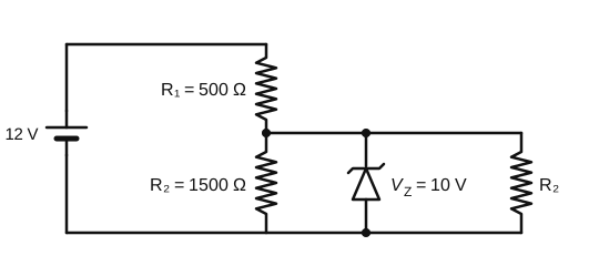
Concept. Check for breakdown first, then use the regulator equations.
Step 1. Without the Zener. $15\times\dfrac{1500}{2000}=11.25$ V $>10$ V: it breaks down, holding $10$ V.
Step 2. Currents. Through $R_1$: $\dfrac{15-10}{500}=10$ mA. Through $R_2$: $\dfrac{10}{1500}=6.67$ mA.
Step 3. Zener current. $10-6.67=3.3$ mA.
Answer. Option A.
Solution by Sreeraj P, M.Sc Physics
Q 12-14-199JEE MainJEE Main 2018 (16 Apr, Shift 1)Easy
A carrier wave of peak voltage $14\ \text{V}$ is used for transmitting a message signal. The peak voltage of the modulating signal given to achieve a modulation index of $80\%$ will be:
When the input (base) voltage rises, the collector current rises, the drop across the load resistor increases and the collector voltage falls. The output is therefore inverted: the phase difference is $180^\circ$.
Solution by Sreeraj P, M.Sc Physics
Q 12-14-201JEE MainJEE Main 2017 (8 Apr)Easy
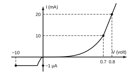
The $V$–$I$ characteristic of a diode is shown in the figure. The ratio of forward to reverse bias resistance is:
The conductivity of a semiconductor sample having electron concentration of $5\times10^{18}\ \text{m}^{-3}$, hole concentration of $5\times10^{19}\ \text{m}^{-3}$, electron mobility of $2.0\ \text{m}^2\text{V}^{-1}\text{s}^{-1}$ and hole mobility of $0.01\ \text{m}^2\text{V}^{-1}\text{s}^{-1}$ is: (Take charge of an electron as $1.6\times10^{-19}$ C)
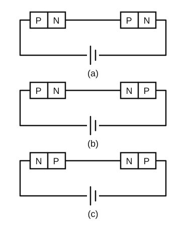
In each circuit the two junctions are in series with the cell.
(a) PN and PN face the same way, so both are forward biased or both reverse biased. They are identical and carry the same current, so the drops are equal.
(c) NP and NP also face the same way: equal drops for the same reason.
(b) PN and NP face opposite ways, so one is forward biased (small drop) and the other reverse biased (almost all the cell voltage). The drops are unequal.
Equal in (a) and (c).
Solution by Sreeraj P, M.Sc Physics
Q 12-14-206NEETNEET 2022Top questionEasy
In half wave rectification, if the input frequency is $60$ Hz, then the output frequency would be
So $C = 1, 0, 1, 0$ for $AB = 00, 01, 10, 11$, which is table (4).
Solution by Sreeraj P, M.Sc Physics
Q 12-14-208JEE MainJEE Main 2025 (2 Apr, Shift 1)Medium
A zener diode with $5\ \text{V}$ zener voltage is used to regulate an unregulated dc voltage input of $25\ \text{V}$. For a $400\ \Omega$ resistor connected in series, the zener current is found to be 4 times the load current. The load current ($I_L$) and load resistance ($R_L$) are:
Concept. In n-type material electrons are majority carriers from pentavalent donors; holes come only from thermal pair generation, and the mass-action law $n_en_h=n_i^2$ still holds.
Step 1. Check. A true; B true; C false; D false (it is equal); E true.
Answer. (A), (B), (E) only (Option C).
Solution by Sreeraj P, M.Sc Physics
Q 12-14-214JEE MainJEE Main 2025 (7 Apr, Shift 1)Medium
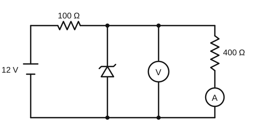
In the circuit shown in the figure, a $12\ \text{V}$ battery is connected through a $100\ \Omega$ resistor to a zener diode (breakdown voltage $4\ \text{V}$), a voltmeter, and a $400\ \Omega$ resistor in series with an ammeter, all three in parallel. The reading of the ammeter will be:
First check whether the zener breaks down. Without it, the $400\ \Omega$ load would get $$V = \frac{400}{100 + 400}\times12 = 9.6\ \text{V} > 4\ \text{V}$$
So the zener conducts and holds the parallel part at $4\ \text{V}$. The ammeter is in series with $400\ \Omega$: $$I = \frac{4}{400} = 0.01\ \text{A} = 10\ \text{mA}$$
Solution by Sreeraj P, M.Sc Physics
Q 12-14-215JEE MainJEE Main 2025 (7 Apr, Shift 2)Medium
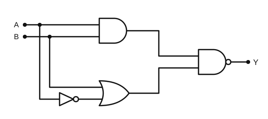
Consider the logic circuit shown in the figure: A and B feed an AND gate; NOT A and B feed an OR gate; the outputs of the AND and OR gates feed a NAND gate whose output is Y. The output is $Y = 0$ when:
$Y_1 = A\cdot B$, $Y_2 = \overline A + B$, and $Y = \overline{Y_1\cdot Y_2}$.
A NAND gate gives 0 only when both its inputs are 1. $Y_1 = 1$ needs $A = B = 1$, and then $Y_2 = 0 + 1 = 1$ as well, so $Y = 0$.
For every other input $Y_1 = 0$, so $Y = 1$. Hence $Y = 0$ only for $A = 1$, $B = 1$.
Solution by Sreeraj P, M.Sc Physics
Q 12-14-216JEE MainJEE Main 2025 (8 Apr, Shift 2)Medium
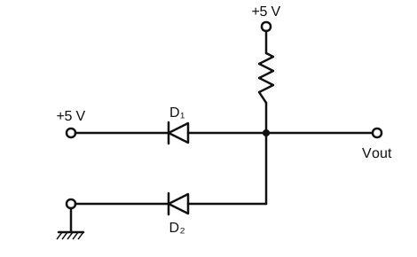
The output voltage in the following circuit is (consider ideal diodes): a $+5\ \text{V}$ supply feeds the output node through a resistor; diode $D_1$ connects the node to a $+5\ \text{V}$ terminal and diode $D_2$ connects the node to ground, both with their anodes at the node, as shown in the figure.
$D_2$ has its anode at the node and its cathode at ground. The node is pulled up through the resistor, so $D_2$ is forward biased and, being ideal, clamps the node to $0\ \text{V}$.
$D_1$ then has $0\ \text{V}$ at its anode and $+5\ \text{V}$ at its cathode: reverse biased, so it carries no current.
The whole $5\ \text{V}$ drops across the resistor and $V_{\text{out}} = 0\ \text{V}$. (This is a diode AND gate with inputs 1 and 0.)


 Solution by Sreeraj P, M.Sc Physics